ITO Conductive Glass | Film Thickness & Sheet Resistance Specs
- Share
- publisher
- Felix Glass Co., Limited
- Issue Time
- Oct 21,2026
Summary
Articles focus on ITO film deposition parameters, resistance consistency, optical transmission balance and batch inspection criteria for transparent conductive glass.
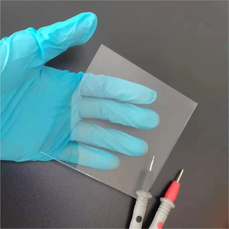
Articles focus on ITO film deposition parameters, resistance consistency, optical transmission balance and batch inspection criteria for transparent conductive glass. ITO conductive glass relies on sputtered indium tin oxide thin films to achieve high electrical conductivity and high visible light transmittance. Sheet resistance is directly determined by film thickness and bulk resistivity. Strict thickness control is the primary method to stabilize resistance across batches, while balancing low resistance with high light transmission remains the core engineering trade-off for touch panel substrates. Felix Glass controls ITO film uniformity and resistance consistency for capacitive touch screens and transparent electrode components. 1. Uneven sputtering power or unstable oxygen flow causes inconsistent deposition rate, leading to thickness drift and resistance fluctuation.
2. Poor substrate pre-cleaning leaves organic contamination; contaminated areas form thinner ITO films with abnormally high resistance.
3. Post-annealing temperature fluctuation: insufficient annealing keeps high resistivity; over-annealing leads to grain overgrowth and film cracking.
4. Substrate warpage during sputtering creates uneven target-to-substrate distance, resulting in thickness gradient across the glass surface. 1. Define target sheet resistance plus tolerance range, rather than only writing film thickness; resistance is the final acceptance index.
2. Specify resistance uniformity across the whole panel and define grid sampling points for four-point probe testing.
3. Clearly mark the required average visible transmittance (400~700 nm) to avoid over-thick ITO layers.
4. Add surface roughness requirement: Ra ≤2 nm to prevent short circuits during subsequent photolithography and etching. Related categories: Touch Panel Glass, Display Cover Glass We produce ITO coated glass with tightly controlled film thickness, sheet resistance uniformity and high optical transmittance, optimized for capacitive touch panels and transparent electrode applications.ITO Conductive Glass
Technical Articles In This Category
ITO Film Thickness & Sheet Resistance Tolerance
Overview
Core Formula: Sheet Resistance vs Film Thickness
Standard Thickness & Resistance Grades for Touch Panels
Tolerance Control Specifications
Process Factors That Break Resistance Consistency
RFQ Specification Writing Guidelines
Browse More Topics
Custom ITO Conductive Glass Manufacturing