Service life improvement vs standard high-OH fused silica optics under continuous DUV load
Summary
High-Purity Low-OH Fused Silica Components for DUV Lithography, Wafer Inspection & Semiconductor UV Processing Systems
Summary
High-Purity Low-OH Fused Silica Components for DUV Lithography, Wafer Inspection & Semiconductor UV Processing Systems
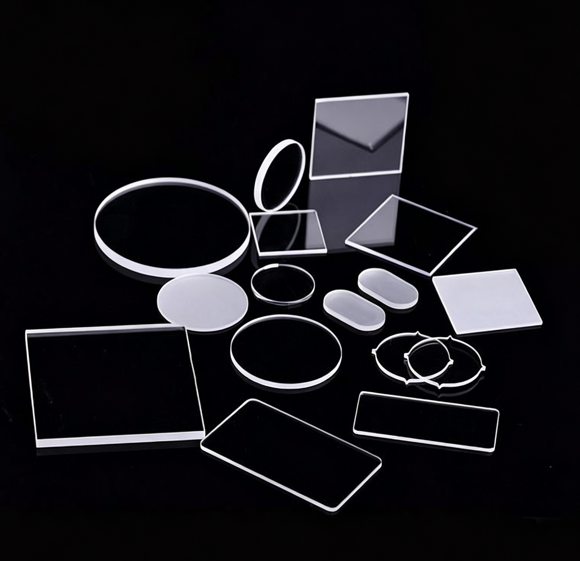
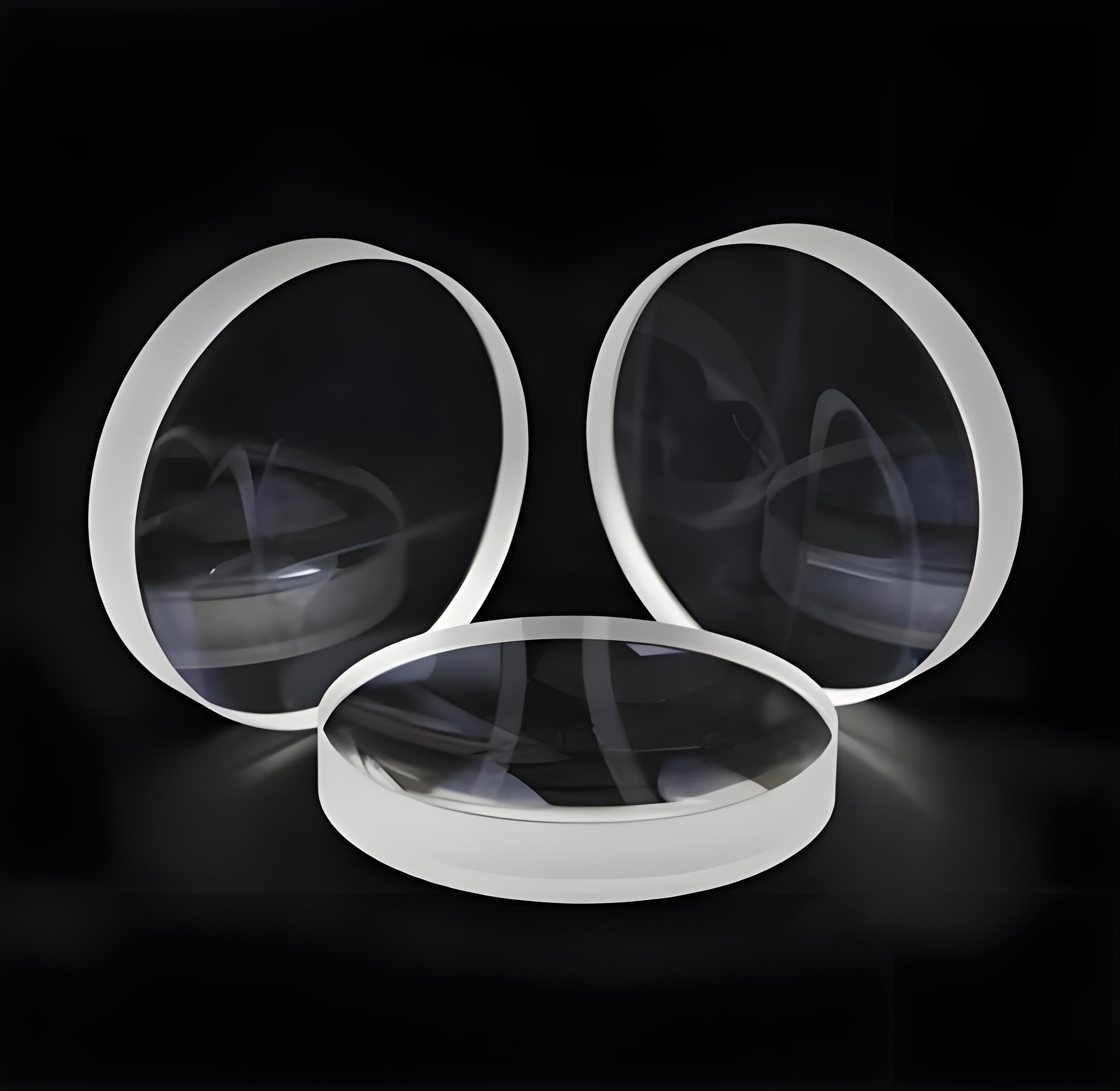
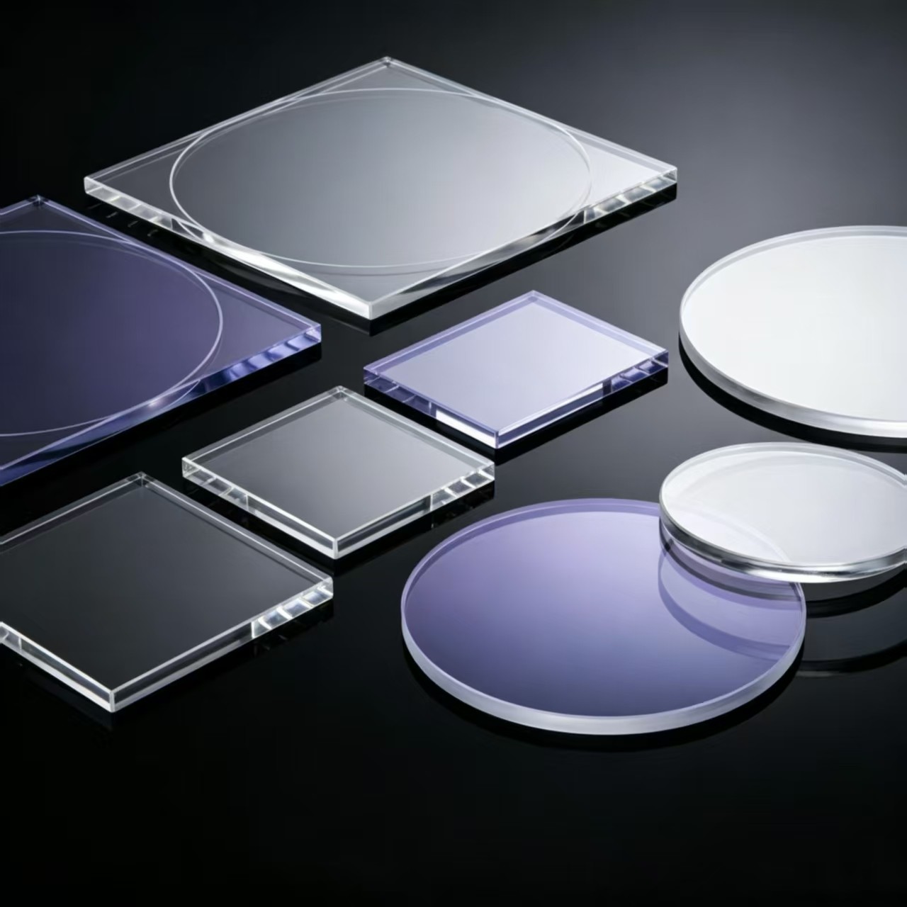
A North American 12-inch wafer fab manufacturer needed DUV optical components that could maintain stable deep-UV transmission through long-duration high-power UV exposure and corrosive plasma etching gas. Felix Glass developed drawing-based low-OH fused silica optical blanks with precision CNC machining and DUV-matched anti-reflection coating for lithography & wafer inspection optical paths. The lithography tool ran continuously under 193–355nm high-power DUV irradiation. The original high-OH fused silica optics lasted roughly two weeks under full production load. Hydroxyl impurities induced strong UV absorption and fluorescence; corrosive plasma etching gas etched uncoated optical surfaces, while generic off-the-shelf quartz blanks could not match the customer’s lithography optical cavity without secondary rework. The client was a North American semiconductor wafer fab operating DUV lithography & wafer UV inspection lines. Its optical design and procurement teams required custom fused silica optics that fit existing lithography optical cavity, resist long-term DUV irradiation & plasma corrosive gas, and maintain high transmittance at 193/248nm deep UV band. The drawing review centered on clear aperture, overall blank dimensions, substrate thickness, edge chamfer, mounting groove, DUV coating wavelength band, and assembly matching tolerance between fused silica optics and optical bench housing. Low-OH ultra-pure fused silica was selected for its balanced deep-UV transmittance, low fluorescence, thermal stability and plasma chemical resistance. Ultra-low hydroxyl raw material eliminates strong UV absorption under long DUV irradiation, critical for consistent wafer patterning precision. Final material selection depends on target DUV wavelength, optical power load, thermal gradient and process plasma chemistry; material grade must be confirmed against full semiconductor equipment specifications. For related material guidance, review the review the fused silica optical glass material and product range. Felix Glass uses the customer’s lithography optical bench drawing to define blank diameter, thickness, edge chamfer and mounting groove geometry. Perfect dimensional matching with installed optical cavity avoids secondary precision grinding and lowers assembly debugging uncertainty for wafer fab R&D teams. For similar semiconductor optical assemblies, see the DUV lithography low-OH fused silica optical window. Low-OH fused silica blanks are engineered to withstand long-hour high-power deep UV irradiation, plus fluorine/chlorine plasma corrosive gas inside etching & lithography chambers. No surface fogging, fluorescence or transmittance decay occurred during the full fab evaluation cycle. Long-term service performance varies based on DUV power density, plasma composition, coating design and routine equipment cleaning procedures. See the related DUV AR-coated fused silica protection window for lithography exposure cameras for full system selection reference. Service life improvement vs standard high-OH fused silica optics under continuous DUV load Stable deep UV transmission after custom DUV AR coating Reduced spare part inventory & equipment downtime maintenance expense Standardized drawing dimensions eliminate on-site secondary grinding work These metrics reflect real feedback from the client’s wafer fab production line and cannot be guaranteed for all DUV semiconductor equipment. Final performance varies with DUV wavelength, optical power, plasma atmosphere, blank geometry and fab maintenance protocols. UV optical blank, lens & window for continuous wafer patterning exposure optical paths High-flatness fused silica viewport for tiny feature wafer surface UV scanning detection Corrosion-resistant DUV optical window for real-time plasma process UV observation Drawing-based custom fused silica optics for UV surface cleaning & chip packaging curing control For additional design context, read the fused silica flatness tolerance and custom CNC machining guide. This project’s low-OH fused silica blank stably works for 185–400nm deep UV band, optimized for 193/248nm DUV lithography. Actual usable wavelength range is limited by coating design, blank thickness and continuous UV power load of the optical system. Ultra-pure fused silica features excellent chemical inertness against fluorine & chlorine plasma; matched DUV AR coating further blocks surface corrosion under long production cycles. We fully support drawing-based CNC precision machining for custom diameter, thickness, groove and chamfer to fit customer’s existing optical cavity without secondary rework. Submit your lithography optical bench CAD drawings, DUV working wavelength & power parameters, plasma chamber atmosphere, target coating transmittance, order quantity and SEMI inspection requirements. Felix Glass optical engineers will review raw material grade, blank geometry, DUV coating scheme and mass manufacturability for custom semiconductor UV fused silica components..
UV SEMICONDUCTOR DUV LITHOGRAPHY Case Study
185–400nm Stable DUV Transmission BandSpecified deep ultraviolet working spectrum for lithography exposure
0.8–15 mm Custom Blank ThicknessCustom substrate thickness for lithography lens & viewport
λ/10 / λ/20 Surface FlatnessSemiconductor-grade interferometer flatness tolerance
5x Extended Service LifeCompared with standard high-OH fused silica optics
Why the Original UV Fused Silica Optics Was Failing
Interest
Client and Application Requirements
Why Low-OH Fused Silica Was Selected
Custom Fused Silica Optics Specification
Substrate Low-OH / Ultra-low OH synthetic fused silica Thickness Custom 0.8–15 mm per lithography drawing Flatness λ/10 / λ/20 @632.8nm semiconductor grade Surface quality 10/5, 20/10 scratch-dig for chip production Coating Double-sided DUV anti-reflection coating matched to 193/248/355nm lithography band Mechanical features CNC chamfer, mounting groove & counterbore machined per optical bench CAD drawing Operating target Stable long-term operation under continuous high-power DUV irradiation, resistant to plasma etching gas environment 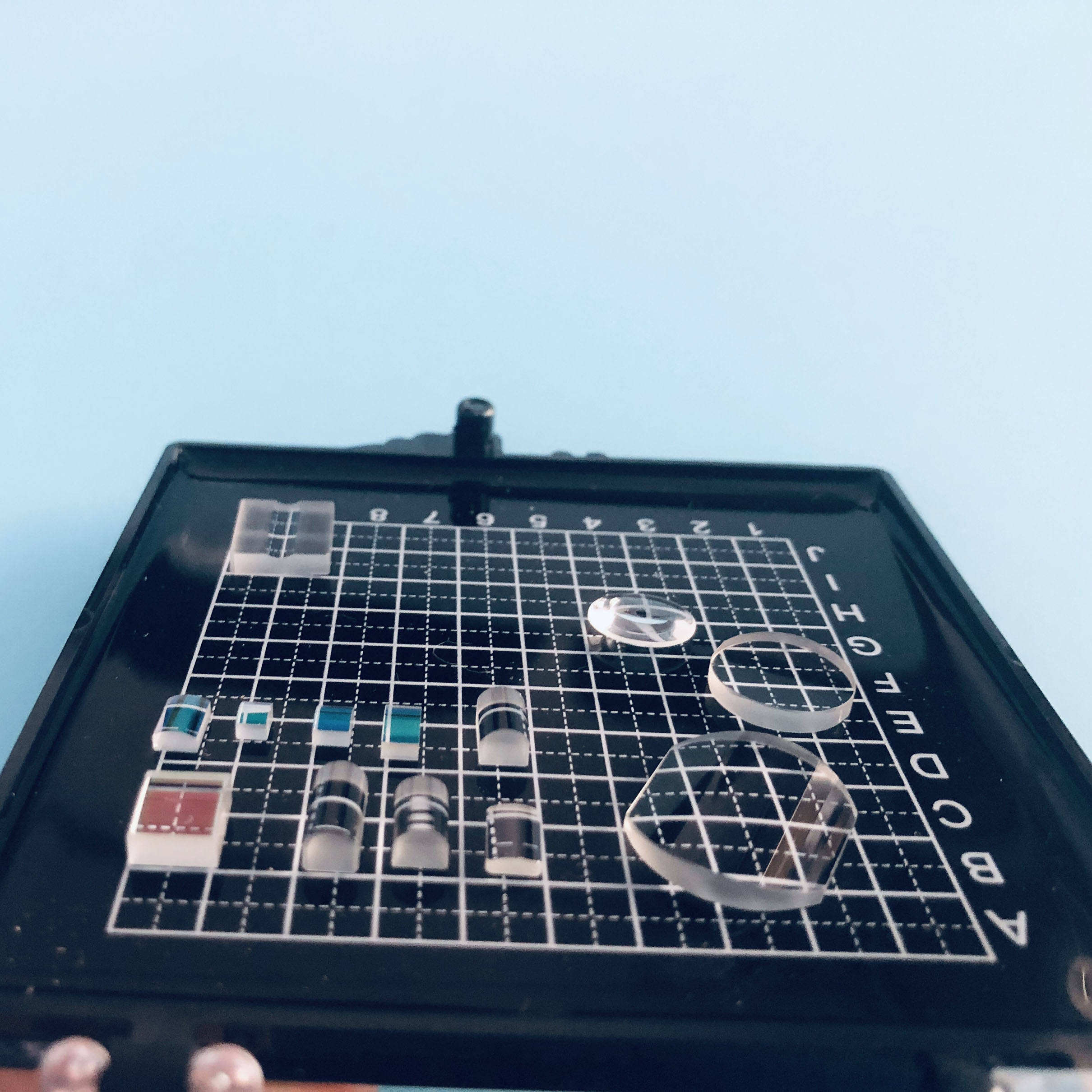
Precision Machining for the Existing Camera Housing
Resistance to DUV Irradiation & Plasma Corrosive Semiconductor Atmospheres
Measured Results from This Furnace Camera Project
Where This Sapphire Viewport Approach Can Be Applied
DUV Lithography Exposure Tools
Wafer UV Inspection & Metrology Equipment
Plasma Etching UV Monitoring Chambers
Semiconductor UV Cleaning & Curing Equipment
Engineering and Procurement Checklist
Semiconductor Optical Design EngineerProvide DUV working wavelength, continuous UV power, plasma chamber atmosphere, target transmittance band and optical bench mounting structure
Wafer Fab Procurement ManagerProvide monthly mass forecast, prototype sample quantity, production delivery schedule, SEMI material certification and export packaging requirements
DUV Optics Component EngineerSupply clear aperture, blank overall dimension, substrate thickness, flatness grade, scratch-dig surface quality, edge chamfer & groove drawing details and DUV AR coating target
Engineering FAQ
Q:What UV wavelength can semiconductor fused silica optics support?
Q:Does low-OH fused silica resist plasma etching corrosive gas inside semiconductor chambers?
Q:Can Felix Glass customize fused silica optics to match existing lithography optical bench housing?
Request a DUV Semiconductor Fused Silica Optics Engineering Review