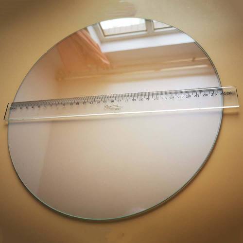
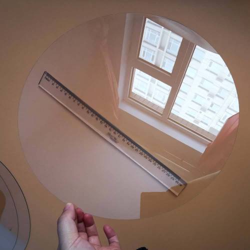
Bare Polished Glass Wafer for Semiconductor Packaging
- Model
- FG-Bare Polished Glass Wafer
Item specifics
- Glass Material
- Alkali-Free Aluminosilicate Glass / Borosilicate Glass
- Substrate Format
- 100 mm, 200 mm, or 300 mm Round Wafers / Custom Panels
- Nominal Thickness
- 100–1,000 µm, depending on glass grade and format
- Surface Finish
- Uncoated, Double-Side Polished (DSP)
- Via Status
- Blank Substrate, No Through-Glass Vias
- Application
- Semiconductor Packaging / TGV Process Development
Review
Description
Bare Polished Glass Wafer for Semiconductor Packaging
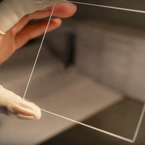
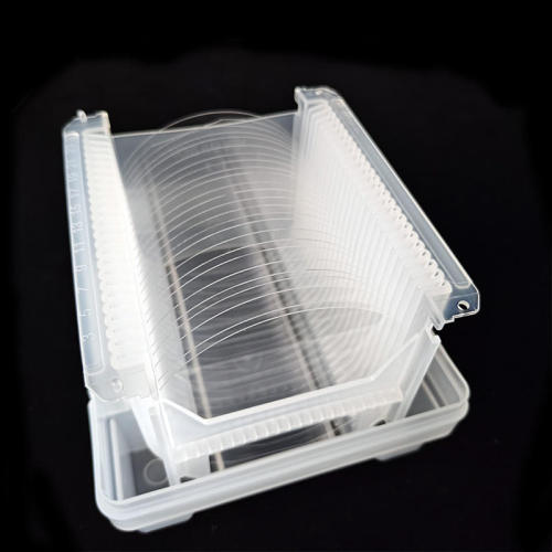
Felix Glass supplies bare, double-side polished glass wafers and custom panels for semiconductor packaging, through-glass via (TGV) process development, and photonics prototyping. These uncoated glass blanks are supplied without vias, metal layers, redistribution layers (RDL), or release coatings. They provide a starting substrate for teams qualifying their own laser drilling, lithography, thin-film deposition, or metallization processes.
Specify the glass grade, wafer or panel dimensions, and inspection limits to match your handling equipment and downstream process.
Wafer Specifications
| Parameter | Specification |
|---|---|
| Glass Material | Alkali-free aluminosilicate glass or borosilicate glass. Specify the required grade if your process is already qualified. |
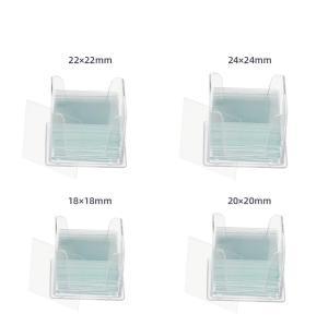
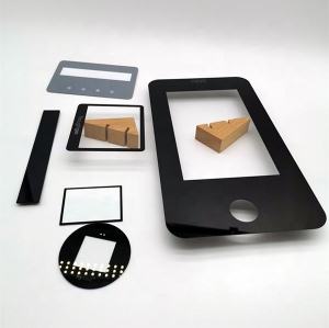
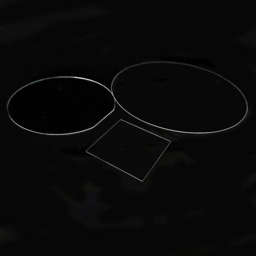
| Format | 100 mm, 200 mm, or 300 mm round wafers. Custom square and rectangular panels are also available for review. |
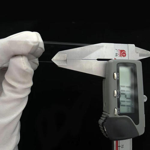
| Nominal Thickness | 100–1,000 µm (0.10–1.00 mm), subject to glass grade and format. Specify the nominal thickness and allowable thickness tolerance. |
| Surface Finish | Uncoated, double-side optical polish (DSP). A target of Ra ≤ 0.5 nm can be reviewed against the requested measurement method and scan area. |
| Total Thickness Variation (TTV) | Specify the maximum TTV in µm and any measurement-area or edge-exclusion requirements. The achievable limit is confirmed for the selected format and thickness. |
| Bow and Warp | Specify allowable bow and warp separately if your tooling or process requires both limits. |
| Edge and Orientation | Include edge profile, notch or flat, and any corner requirements on your drawing where applicable. |
Availability and acceptance limits are confirmed for the requested combination of glass grade, size, and thickness.
Choosing a Glass Grade
Alkali-free aluminosilicate glass. Consider this option when your process specifies an alkali-free substrate. For assemblies that include silicon, compare the selected grade’s coefficient of thermal expansion (CTE) with the assembly requirements over the actual process temperature range.
Borosilicate glass. Consider this option when the selected grade meets the thermal and bonding requirements of your process. For glass-to-silicon anodic bonding, specify the bonding method and temperature so the grade can be reviewed for that process.
For RF or photonic builds, share the operating frequency or wavelength and the required dielectric or optical properties. This allows the review to focus on the specific glass grade.
Typical Applications
- TGV development: Laser drilling trials, via geometry studies, and process qualification coupons.
- Advanced packaging: Fan-out process trials and evaluation of glass substrates for interposer or glass-core development.
- Thin-film process development: Lithography, sputtering, and qualification of dielectric, adhesion, or barrier layers.
- Photonics prototyping: Glass substrate evaluation for optical waveguide and photonic integration projects.
Inspection and Packaging
Pre-shipment inspection covers dimensions, TTV, warp, and visible surface defects such as scratches and digs. Include any specific measurement method, surface-defect limits, or inspection report requirements in your RFQ so they can be confirmed before ordering. Specify your preferred wafer shipper, individual wafer packaging, or particulate acceptance criteria if required for incoming inspection.
Related Glass Substrates and Design Guides
- Laser-drilled TGV glass wafer for projects that require vias before in-house metallization.
- Copper-filled TGV glass interposer for projects that require conductive vias.
- Temporary release glass carrier for fan-out wafer-level and panel-level packaging.
- Glass-core substrate for FC-BGA packaging.
- TGV glass substrate for co-packaged optics.
- TGV glass interposer selection guide.
- TGV wafer and interposer design specifications.
Frequently Asked Questions
- What is the difference between thickness tolerance and TTV?
- Thickness tolerance specifies the permitted deviation from the nominal thickness under the agreed measurement method. TTV is the difference between the thickest and thinnest measured points on one wafer. List both values if both affect your process.
- Can I request a custom panel or a small sample lot?
- Yes. Send your target dimensions, glass grade, and sample quantity. We will review the format and confirm sample availability, minimum order quantity, and lead time.
Request a Quote or Samples
Send your drawing or specification with the glass grade, diameter or panel size, nominal thickness and tolerance, maximum TTV, and required quantity. Include any roughness, bow or warp, edge, inspection, or packaging requirements that affect acceptance. If the glass grade is open, tell us your downstream process and peak process temperature.
Request a Quote