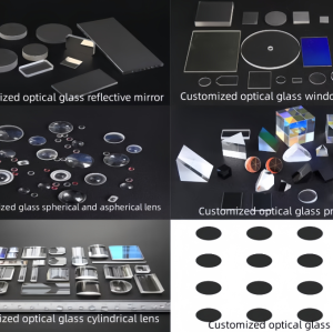
Quartz Wafer Manufacturer | Fused Silica Wafers for Semiconductor, Photolithography & UV Optics
- Model
- FG-QT-005
Item specifics
- Material
- High‑Purity Fused Silica (Amorphous SiO₂)
- SiO₂ Purity
- ≥99.99%
- Diameter
- 2″, 3″, 4″, 6″, 8″, 12″ (custom available)
- Thickness
- 0.1 mm – 5 mm (custom thickness)
- TTV (Total Thickness Variation)
- ≤5 μm (high precision ≤1 μm)
- Surface Quality
- 60/40, 40/20, 20/10 (MIL‑STD)
- Surface Roughness (Ra)
- ≤1 nm (DSP), ≤2 μm (lapped)
- Optical Flatness
- λ/2, λ/4, λ/10 @ 633 nm
- Parallelism
- <30 arcsec
- Transmittance Range
- 185 nm – 3500 nm
- Average Transmittance
- >90%
- Thermal Expansion Coefficient
- 5.5 × 10⁻⁷ /°C
- Instant Temp Resistance
- 1300°C
- Available Finishes
- DSP (double‑side polished), SSP (single‑side polished), lapped
- Optional Features
- Notch, flat edge, drilling, coating (AR/UV/IR)
Review
Description
Quartz Wafer Manufacturer | Fused Silica Wafers for Semiconductor & Optics
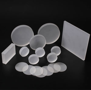
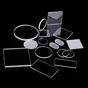
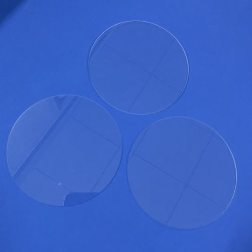
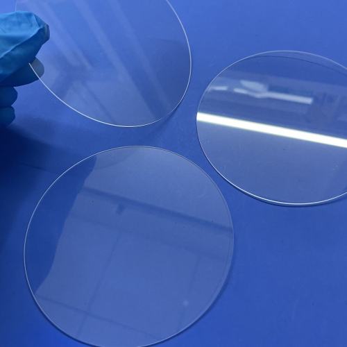
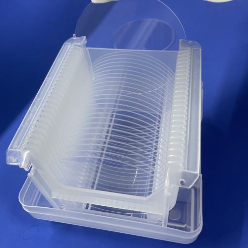
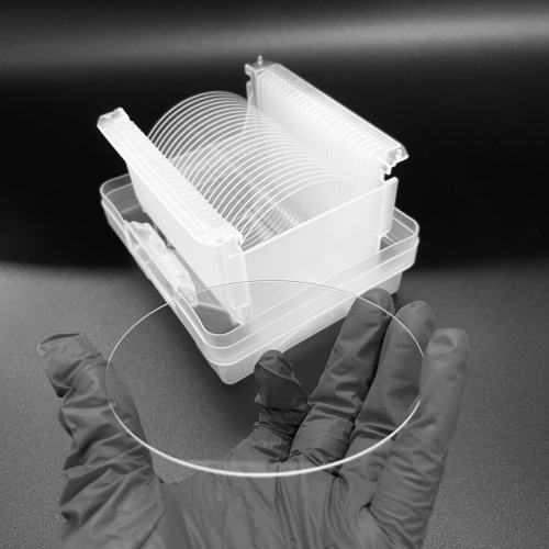
Felix Glass is a professional quartz wafer manufacturer and supplier specializing in high-purity fused silica wafers for semiconductor, photolithography, UV optics, MEMS and laboratory applications. Produced from ≥99.99% SiO₂ fused quartz, our quartz wafers deliver ultra-low thermal expansion, exceptional UV–IR transmittance, high surface flatness and outstanding chemical stability.
Available in JGS1, JGS2 and JGS3 grades, with single‑side polished (SSP) or double‑side polished (DSP) finishes, our wafers support 2″–12″ diameters and ultra‑thin profiles down to 0.1 mm, meeting strict MIL‑STD and semiconductor‑level precision requirements.
Technical Specifications
| Property | Value |
|---|---|
| Material | High‑Purity Fused Silica (Amorphous SiO₂) |
| SiO₂ Purity | ≥99.99% |
| Diameter | 2″, 3″, 4″, 6″, 8″, 12″ (custom available) |
| Thickness | 0.1 mm – 5 mm (custom thickness) |
| TTV (Total Thickness Variation) | ≤5 μm (high precision ≤1 μm) |
| Surface Quality | 60/40, 40/20, 20/10 (MIL‑STD) |
| Surface Roughness (Ra) | ≤1 nm (DSP), ≤2 μm (lapped) |
| Optical Flatness | λ/2, λ/4, λ/10 @ 633 nm |
| Parallelism | <30 arcsec |
| Transmittance Range | 185 nm – 3500 nm |
| Average Transmittance | >90% |
| Thermal Expansion Coefficient | 5.5 × 10⁻⁷ /°C |
| Continuous Working Temp | 1100°C |
| Instant Temp Resistance | 1300°C |
| Available Finishes | DSP (double‑side polished), SSP (single‑side polished), lapped |
| Optional Features | Notch, flat edge, drilling, coating (AR/UV/IR) |
Product Types
JGS1 Deep UV Quartz Wafer
- Wavelength: 185 nm – 2500 nm
- Features: Superior deep‑UV transmittance, low OH content
- Applications: Excimer laser, photolithography (193 nm), DUV sterilization, semiconductor mask substrates
JGS2 General UV Quartz Wafer
- Wavelength: 220 nm – 2500 nm
- Features: Cost‑effective, high uniformity
- Applications: UV curing, optical windows, laboratory substrates, MEMS, inspection systems
JGS3 Infrared Quartz Wafer
- Wavelength: 260 nm – 3500 nm
- Features: Excellent IR transmission, high‑temperature stability
- Applications: IR imaging, thermal sensing, high‑temp process wafers, aerospace optics
Key Features
Ultra‑High Purity & Low Defects
- ≥99.99% SiO₂, minimal bubbles, inclusions or striae
- Low metal impurities, ideal for high‑cleanliness semiconductor processes
Superior Thermal Stability
- Near‑zero thermal expansion, resistant to thermal shock and cycling
- Stable at 1100°C continuous, 1300°C instant
Excellent UV–IR Transmission
- High transmittance from deep UV to mid‑IR
- Critical for photolithography, laser and IR systems
High Precision & Flatness
- TTV ≤1 μm available; λ/10 flatness for high‑end optics
- DSP polishing (Ra <1 nm) for mask and wafer bonding applications
Chemical Inertness
- Resists acids, alkalis and most solvents
- Compatible with semiconductor wet processing
Applications
- Semiconductor photolithography mask substrates
- Wafer‑level packaging (WLP) & MEMS
- UV laser systems & excimer laser optics
- High‑temperature process chambers & dummy wafers
- Infrared imaging & thermal sensing components
- Laboratory analytical instruments & optical metrology
- Aerospace & defense optical windows
- Photomask blanks & EUV/UV optics
Custom Manufacturing Services
Felix Glass provides full OEM/ODM quartz wafer solutions:
- Custom diameters (2″–12″) & thicknesses (0.1 mm+)
- DSP/SSP polishing, lapping & edge treatment (notch/flat)
- Precision drilling, slotting & micro‑machining
- AR, UV anti‑reflection & IR transmission coatings
- Tight TTV/flatness tolerances for semiconductor grades
- Small prototypes & mass production supported
Why Choose Felix Glass
- Professional quartz wafer manufacturer with 15+ years export experience
- ISO 9001 certified, strict MIL‑STD & semiconductor‑grade QC
- Full JGS1/JGS2/JGS3 product line, high consistency
- Advanced polishing & metrology (interferometer, surface profiler)
- Fast sampling, short lead time & stable bulk supply
- Global delivery for EU/US semiconductor & optical clients
FAQ
What is a quartz wafer?
A quartz wafer is a thin, flat fused silica disc made of high‑purity SiO₂, precision polished for semiconductor, optical and MEMS applications。
Quartz wafer vs. silicon wafer — key difference?
Quartz offers UV transparency, much lower thermal expansion and better high‑temp stability; silicon is opaque in UV and has higher CTE。
What grades do you offer?
JGS1 (deep UV)、JGS2 (general UV)、JGS3 (infrared)。
What sizes are available?
Standard 2″, 3″, 4″, 6″, 8″, 12″; custom diameters on request。
Do you provide double‑side polished (DSP) wafers?
Yes. DSP (Ra <1 nm) and SSP options available。
What is TTV?
Total Thickness Variation — smaller values (≤1 μm) mean higher thickness uniformity, critical for lithography。
Can you make ultra‑thin quartz wafers?
Yes, down to 0.1 mm thickness with strict tolerances。
Are coatings available?
Yes: AR, UV and IR coatings。
Do you support semiconductor‑level quality?
Yes, with low TTV, high flatness, low defects and documented inspection reports。
Can I get samples?
Yes, samples available for qualification before volume production。
Related Products
Link: Quartz Glass Plate
Link: Quartz Glass Tube
Request a Quote
Contact Felix Glass today for free technical consultation, custom quartz wafer solutions and factory pricing. Our engineering team supports your semiconductor, photolithography and optical projects worldwide.