Products · Custom ITO Conductive Glass
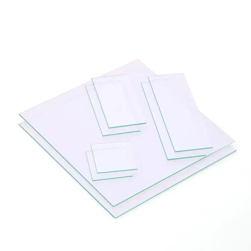
Lab ITO Conductive Slide Electrodes
Custom transparent conductive substrates for laboratory research
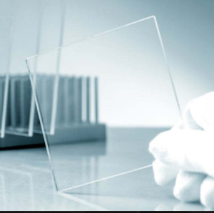
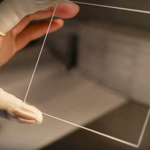
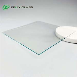
Custom ITO-coated glass slides for research, electrochemical studies and thin-film development, with defined geometry, sheet resistance and optical requirements.
View Slide Specifications1. Transparent Conductive Substrates for Laboratory Projects
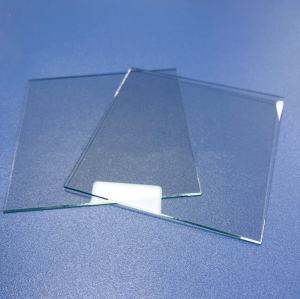
Felix Glass supports custom ITO-coated glass slide electrodes for research and device-development projects requiring optical access and an electrically conductive surface. Indium tin oxide forms the conductive layer on a specified glass substrate.
Select the slide geometry, substrate, coating coverage and electrical targets around your experiment or fabrication process. Finished specifications and inspection scope are confirmed for each project rather than inferred from a generic slide designation.
2. Custom Slide Specification Overview
| Parameter | Specification basis |
|---|---|
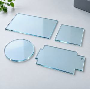
| Format | Rectangular slides, square coupons or custom outlines |
| Dimensions | Length, width, thickness and tolerances to drawing |
| Substrate | Soda-lime, borosilicate or fused silica grade subject to review |
| Coating coverage | Specified conductive face, full-area coating or defined exclusions |
| Sheet resistance | Target, tolerance and uniformity in Ω/□ |
| Transmission | Finished-substrate spectrum at stated wavelengths |
| Film thickness | Specified where needed; electrical and optical targets also required |
| Active region | Exposed area, immersion boundary and contact zone to drawing |
| Patterning | Isolation gaps, pads and tracks evaluated from artwork |
| Delivery condition | Cleaning, coated-side identification, packaging and reports by agreement |
Provide the holder opening and clamping arrangement when dimensional compatibility is critical. Standard-looking slide dimensions do not establish interchangeability with every laboratory fixture.
3. Choose the Glass Substrate
Soda-lime glass can be considered for general laboratory substrates. Borosilicate or appropriate fused-silica grades may be considered where thermal, chemical or spectral requirements justify them.
Specify the optical band, downstream process temperatures and sensitivity to substrate-derived contamination. Where an alkali barrier is required, identify it explicitly and evaluate the complete layer stack. The substrate and conductive coating must both suit the process.
4. Specify Sheet Resistance and Uniformity
Sheet resistance in Ω/□ describes lateral conduction in the film. Specify the target range and allowed variation across the working region, together with measurement conditions and sampling locations.
A two-probe resistance measurement includes contact effects and depends on probe placement. It is not automatically a sheet-resistance measurement. Agree on a suitable method, including geometry corrections where needed, for acceptance data.
Film thickness alone does not guarantee a particular resistance. Deposition conditions and film properties also matter, so specify the functional electrical target directly.
5. Define Optical Transmission
Provide the source or detector band and a minimum or average transmission requirement. State whether the result includes the glass substrate, and whether the reference is air or an uncoated substrate.
A transmission value at one visible wavelength does not establish UV or near-infrared performance. For spectroscopy, request the spectral interval, measurement resolution and baseline definition that your method requires. Reflection, haze or fluorescence can be specified separately when relevant.
6. Identify the Conductive Face
State whether one face or both faces must be coated. Coated-side identification can be specified through packaging orientation, a nonfunctional-edge mark or another agreed method.
During incoming checks, use an approved contact method outside the active region. Sharp probes or repeated contact on the experimental area can damage a thin film. Do not identify the coated face by scratching the surface or relying only on reflected color.
7. Separate Active Area from Slide Area
The active electrode area is the region exposed to the experiment or defined by the device pattern; it is not necessarily the full slide area. Identify gasket openings, immersion depth, masked zones and contact pads on the drawing.
For reported current density, specify the area convention used. Geometric exposed area and electrochemically active surface area are different quantities. Control the exposure boundary and fixture placement when comparing samples or batches.
8. Contacts, Clips and Patterned Options
Provide the contact-pad location, clip footprint and any restrictions on contact materials. Keep contact arrangements compatible with the experimental medium and avoid unintended exposed conductors in the active region.
For patterned slides, send dimensioned artwork showing conductive regions, isolation gaps, alignment features and pad positions. Track resistance, electrical isolation and residual conductive bridges should be included in the acceptance plan where relevant.
Confirm whether supply includes only the coated slide or additional contacts, deposited pads, leads or assembly. Patterning limits and contact processes are reviewed against the drawing.
9. Electrochemical and Spectroelectrochemical Use
ITO-coated slides can serve as planar working-electrode substrates in suitable electrochemical and spectroelectrochemical arrangements. They are also useful when optical measurements must be made through a conductive interface.
Compatibility depends on electrolyte, solvent, pH, applied potential, reference-electrode convention, temperature and exposure time. Do not assume that ITO is chemically inert or that one universal potential window applies to every experiment.
Validate the blank substrate under your intended conditions and separate substrate response from the response of any deposited functional layer. Specify immersion and sealing requirements with the cell design.
10. Thin-Film and Optoelectronic Research
ITO glass substrates can be evaluated for thin-film deposition, photovoltaic and OLED research, optical sensing and other device-development tasks. The coating acts as one part of a larger device stack.
Include surface texture, cleanliness, pattern layout and any electrical-contact constraints that affect subsequent deposition. Device efficiency, lifetime or yield depends on the complete fabrication process and is not established by slide resistance alone.
11. Cleaning and Surface Preparation
Agree on the delivery cleanliness and any required pre-treatment. Cleaning chemistry, ultrasonic treatment, plasma or UV-ozone exposure can affect the film or subsequent interfaces and should be validated for the selected substrate stack.
If the laboratory will apply its own preparation procedure, request an appropriate as-delivered condition and keep that procedure controlled across samples. Specify residues or contaminants of concern rather than using “clean” as the only acceptance criterion.
Handle slides by approved edge or holder locations and protect the working surface from contact. Storage conditions and packaging should support the intended cleanliness requirement.
12. Thermal Processing and Reuse
Provide the complete thermal history, including ramp rates, dwell times, atmosphere and cooling conditions, when slides will undergo annealing or other heated processing. A glass temperature limit does not automatically establish coating stability or contact compatibility.
Where performance after treatment matters, specify post-process resistance, transmission and adhesion checks. Reuse should be validated against the experiment: a slide that still conducts may have altered surface chemistry, contamination or local damage.
13. Inspection, Packaging and RFQ Requirements
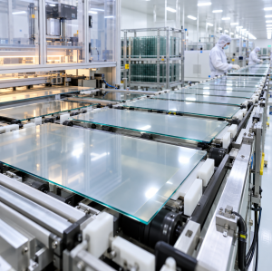
Requested inspection can include dimensions, surface condition, sheet-resistance mapping, coating coverage and spectral transmission. Patterned parts may also need continuity and isolation checks. Agree on methods, sampling and report format before ordering.
Specify protective separation between slides, coated-side identification, lot labels and any cleanliness requirements. Prototype and production quantities are quoted separately, with lead time and documentation scope confirmed for the project.
14. Frequently Asked Questions
Are these microscope slides or electrode substrates?
They are conductive glass substrates. Compatibility with a microscope, cell or holder depends on the specified dimensions, optical properties and fixture requirements.
Does the entire slide count as active electrode area?
Only if the experiment actually exposes and uses that entire region. Define the active area through the cell, mask or device pattern.
Is sheet resistance the same as clip-to-clip resistance?
No. Clip-to-clip resistance also depends on path geometry and contact resistance.
Can I request custom sizes or patterns?
Yes. Submit a dimensioned drawing and pattern artwork for feasibility and quotation.
Can the slides be used with any electrolyte?
No universal compatibility applies. Validate the coating in the intended chemistry, potential range, temperature and exposure time.
Is a single transmission percentage sufficient?
Only if it fully defines your optical requirement. Spectroscopy and broadband applications generally require a defined spectrum or band.
Are the slides sterile or approved for clinical use?
No such claim is implied by laboratory use. Sterility, biological compatibility or regulated-use requirements need a separately agreed specification and validation scope.
What reports can be requested?
Dimensional, electrical and optical data can be discussed. Confirm methods, sampling, traceability and whether results are lot-specific or part-specific in the quotation.
15. Request Lab ITO Slide Electrodes
Send your slide drawing, experiment or device requirements, electrical targets and quantities to Felix Glass. If the design is not finalized, identify the holder dimensions, optical band and process conditions for a focused technical review.
Dongguan Felix Glass Co., Ltd.
Email: james@felixglass.com