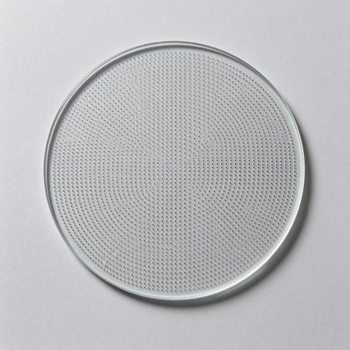
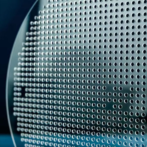

Laser Drilled TGV Glass Wafer (Drill Only, No Metallization)
Item specifics
- Glass Material
- Alkali-Free Aluminosilicate Glass / Borosilicate Glass
- Substrate Format
- 100 mm, 200 mm, or 300 mm Round Wafers / Custom Square Panels
- Nominal Thickness
- 100–1,000 µm, depending on glass grade and format
- Via Spec
- Via Diameter 20–200 µm; Minimum Pitch ≥50 µm; Aspect Ratio up to 10:1
- Delivered Condition
- Laser-Drilled and Cleaned Open Vias, No Metallization or Copper Fill
- Application
- Semiconductor Packaging / TGV Metallization Development
Review
Description
Laser-Drilled TGV Glass Wafer (Drill Only, No Metallization)
Felix Glass supplies laser-drilled through-glass via (TGV) wafers and custom glass panels for advanced packaging development. The glass is delivered with open through-holes and cleaned after drilling. The drill-only scope excludes dielectric liners, barrier and seed layers, copper fill, redistribution layers (RDL), and post-fill planarization.
Use this substrate when your team needs a custom via layout and will qualify its own thin-film deposition, electroplating, or metallization process. Send the substrate dimensions and via layout so we can review the geometry before quoting samples.
TGV Wafer Specifications
| Parameter | Specification or Design Input |
|---|---|
| Base Glass Material | Alkali-free aluminosilicate glass or borosilicate glass. Specify the exact grade if your process requires one. |
| Substrate Format | 100 mm, 200 mm, or 300 mm round wafers. Custom square panels are available for review. |
| Nominal Glass Thickness | 100–1,000 µm (0.10–1.00 mm), subject to glass grade, format, and via geometry. |
| Via Diameter | 20–200 µm for engineering review. Specify entrance and exit diameters, their tolerances, and the minimum internal diameter if critical. |
| Via Pitch | Center-to-center pitch from 50 µm, subject to layout review. Include the minimum glass spacing between adjacent holes and the via-to-edge clearance where critical. |
| Via Aspect Ratio | Up to 10:1 for engineering review. Specify which via diameter is used to calculate the thickness-to-diameter ratio, especially for tapered vias. |
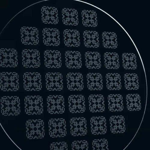
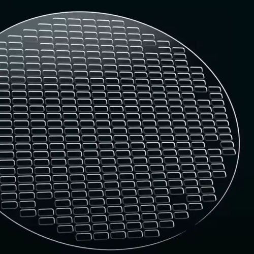
| Via Profile and Position | Custom arrays and non-uniform layouts are reviewed against your drawing. Include the positional tolerance, datum, and any taper limit. |
| Delivered Condition | Drilled and cleaned glass with open, unfilled, unmetalized through-vias. |
The ranges are reviewed together. Feasibility depends on the glass grade, thickness, via diameter and profile, pitch, and array layout.
Via Design for Downstream Metallization
For deposition or plating trials, provide the required entrance, exit, and minimum internal diameters along with the allowable taper. If your process requires a specific deposition direction, identify the corresponding wafer face on the drawing. This gives us the geometry needed to review the drilled substrate against your process requirements.
For dense or irregular arrays, include the smallest local pitch, allowable via position error, and edge clearance. If the layout and drawing are separate files, identify the governing revision and drawing units.
Post-Drill Cleaning and Inspection
Post-drill cleaning removes drilling debris from wafer surfaces and via openings. Agree on the inspection scope and acceptance limits before ordering. Typical inspection items include via diameter and position, visible edge chipping, sidewall condition, residual debris, substrate dimensions, total thickness variation (TTV), and warp.
If your qualification plan requires cross-section sampling or an inspection report, specify the sample locations, measurement method, and report contents in the RFQ. Include any wafer shipper or particulate acceptance requirements that apply to incoming inspection.
Typical Applications
- TGV liner, barrier, seed-layer, and copper electroplating qualification.
- 2.5D packaging test vehicles for chiplet and high-bandwidth memory (HBM) development.
- Via layout and manufacturability trials for glass-core and fan-out packaging.
- Glass substrate prototypes for co-packaged optics (CPO) and photonic packaging.
Related Glass Substrates and Design Guides
- Bare polished glass wafer for teams that perform via drilling in-house.
- Copper-filled TGV glass interposer for designs that require conductive vias.
- Temporary release glass carrier for fan-out wafer-level and panel-level packaging.
- Glass-core substrate for FC-BGA packaging.
- TGV glass substrate for co-packaged optics.
- TGV wafer and interposer engineering design specifications.
- TGV glass interposer selection guide.
Frequently Asked Questions
- Can you review an irregular or mixed-pitch via layout?
- Yes. Send your dimensioned drawing or Gerber layout with the via sizes, pitch, datums, and edge clearances. Feasibility is reviewed for the complete layout.
- Can I specify sidewall taper and request a cross-section?
- Yes. Include the target entrance and exit diameters or the allowable taper, along with the glass thickness and tolerance. Cross-section sampling can be requested for qualification.
- Can I order samples before committing to a production lot?
- Submit your drawing and target sample quantity. We will confirm sample availability, acceptance criteria, and lead time after reviewing the design.
Request a TGV Drilling Quote
Send your via layout, glass grade, wafer or panel size, nominal thickness, via diameters, minimum pitch, and sample or production quantity. Include any critical taper, positional tolerance, or inspection requirements for engineering review.
Request a Quote