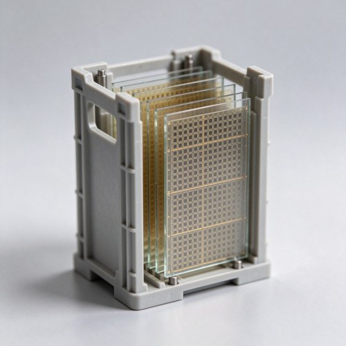
Glass Core Substrate for High-End FC-BGA Packaging
- Model
- FG-FC-BGA Substrate Build-Up
Item specifics
- Core Material
- Alkali-Free Aluminosilicate Glass
- Substrate Format
- Custom Rectangular Panels / Round Wafers on Request
- Nominal Thickness
- 100–800 µm, depending on format and design review
- Standard Delivery
- Undrilled, Double-Side Polished Glass Core Blank
- Optional TGV
- Laser-Drilled Open Vias or Copper-Filled Vias, Subject to Design Review
- Application
- High-End FC-BGA AI Accelerator and Heterogeneous Packaging
Review
Description
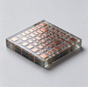
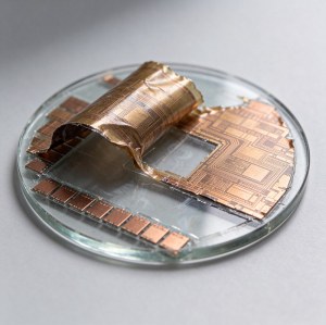
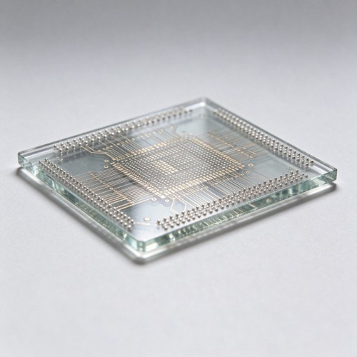
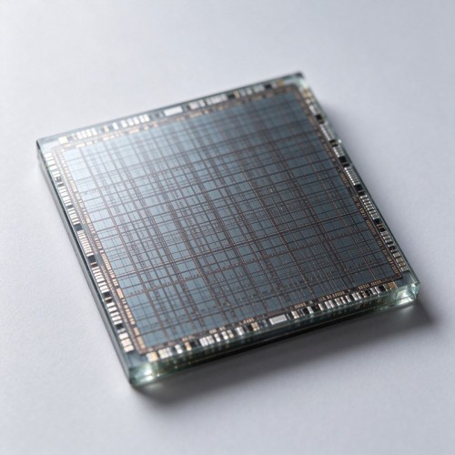
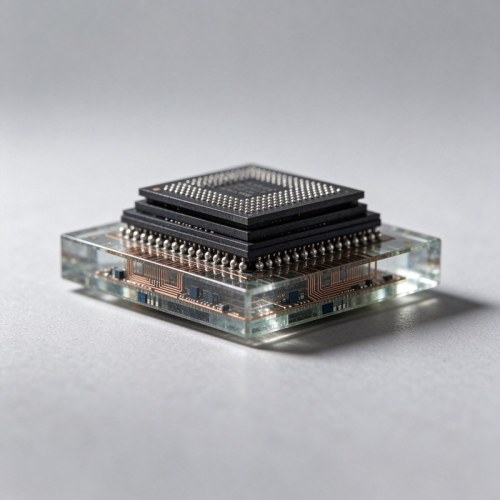
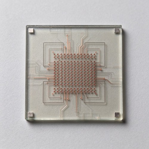
Patterned Glass Core Substrate for FC-BGA Packaging
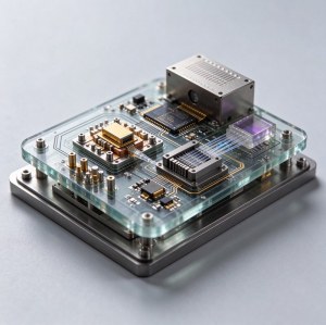
Felix Glass supplies patterned glass core substrates for flip-chip ball grid array (FC-BGA) packaging. The glass core carries circuit patterns and pad features defined by the substrate layout. This product is intended for substrate manufacturers and packaging teams developing multi-die packages, AI accelerators, networking ASICs, and other high-I/O devices.
Send your circuit layout and layer stack for a review of the panel dimensions, patterned faces, pad geometry, and required processing. The quoted configuration defines which layers and features are included at delivery.
Product Specifications
| Parameter | Specification or Design Input |
|---|---|
| Core Glass Material | Alkali-free aluminosilicate glass. Specify the required grade or coefficient of thermal expansion (CTE) range if defined in your stack-up. |
| Nominal Glass Core Thickness | 100–800 µm for design review, subject to panel size and processing requirements. State the glass core thickness separately from any finished substrate thickness requirement. |
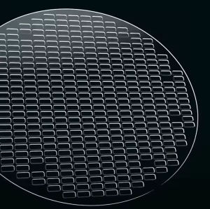
| Substrate Format | Custom rectangular panels. Round wafer formats can be reviewed on request. Include panel or wafer dimensions, tolerances, and any edge clearance requirements. |
| Circuit Pattern and Pads | Provide the required patterned faces, conductor material and thickness, minimum line width and spacing, pad dimensions, and registration tolerances. |
| Dielectric Build-Up and Finish | Specify any required ABF or other dielectric, layer sequence, layer thicknesses, and pad finish. The layer stack and finished condition are confirmed during quotation. |
| Through-Glass Vias (TGVs) | If required, provide the via map, diameters, pitch, and desired via condition. Open or copper-filled via configurations are subject to design review. |
| Dimensional Acceptance | State the applicable thickness tolerance, total thickness variation (TTV), and flatness or warp limits. Identify the processing stage and measurement conditions for each limit. |
Circuit Layout and Stack-Up Review
For panelized layouts, include the overall panel dimensions, unit layout, alignment marks, edge keep-out zones, and drawing revision. Identify the top and bottom faces on the drawing. If your design has patterns on both faces or uses TGVs, specify the required registration between the patterns and via locations.
For lamination or reflow qualification, provide the dielectric stack, copper distribution, and thermal profile. State any finished-substrate warpage limit together with the measurement temperature and method. For high-speed routing, include the target impedance or operating frequency range if it affects the stack-up review.
Typical Applications
- Patterned glass core substrate development for high-I/O FC-BGA packages.
- Routing and pad layout development for AI accelerator and multi-die packages.
- Substrate evaluation for networking ASICs and switch devices.
- Test vehicles for pattern registration, dielectric build-up, and vertical interconnect qualification.
Inspection and Packaging
Define the inspection requirements for the agreed delivery configuration. These can include panel dimensions, circuit feature dimensions and registration, pad condition, surface defects, and flatness or warp. If the order requires electrical continuity testing, via cross-sections, or a lot inspection report, specify the test method, sampling plan, and acceptance limits in your RFQ. Packaging can be reviewed to protect the patterned surfaces during shipment and handling.
Frequently Asked Questions
- Does the substrate ship with a circuit pattern?
- Yes. This product is a patterned glass core substrate. The drawing and quotation define the circuit layout, patterned faces, conductor material, and pad finish for the order.
- Can I specify ABF build-up layers or copper-filled vias?
- Submit the layer stack and via map for review. Include the requested dielectric, via dimensions, and fill acceptance criteria. Any build-up or via processing included at delivery will be listed in the quotation.
- What files should I send for a sample quote?
- Send the dimensioned substrate drawing, circuit layout, and layer stack with matching revision numbers. Include sample quantity, critical tolerances, and any inspection reports needed for qualification.
Related Glass Products and Design Guides
- Bare polished glass wafer for teams developing their own patterning or via processes.
- Laser-drilled TGV glass wafer with open vias for in-house metallization.
- Copper-filled TGV glass interposer for designs requiring conductive vertical interconnects.
- Temporary release glass carrier for fan-out wafer-level and panel-level processing.
- Photonic TGV glass substrate for co-packaged optics.
- TGV wafer and interposer engineering design specifications.
- TGV glass interposer selection guide.
Request a Patterned Glass Core Quote
Send your circuit layout, glass core dimensions and thickness, layer stack, and target quantity. Include any critical line and space, pad, registration, via, or inspection requirements. We will review the requested delivery configuration and confirm sample feasibility, pricing, and lead time.
Request a Quote