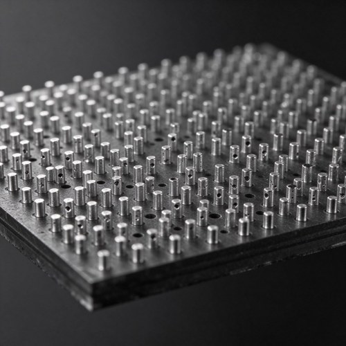
Copper Filled TGV Glass Interposer for AI GPU & HBM 2.5D Heterogeneous Packaging
Item specifics
- Glass Material
- Alkali-Free Aluminosilicate Glass / Borosilicate Glass
- Substrate Format
- 100 mm, 200 mm, 300 mm Wafer / Custom Panel Sizes
- Nominal Thickness
- 100–700 µm
- Via Spec
- Via Diameter 20–120 µm; Pitch ≥50 µm; Aspect Ratio up to 10:1
- Metallization
- Dielectric Liner / Ti Barrier / Cu Seed / Void-Free Electroplated Copper Fill, CMP Planarized
- Application
- AI GPU, HBM Stacks, High-Speed ASIC and 2.5D Heterogeneous Packaging
Review
Description
Copper Filled TGV Glass Interposer for AI GPU & HBM 2.5D Heterogeneous Packaging
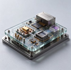
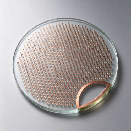
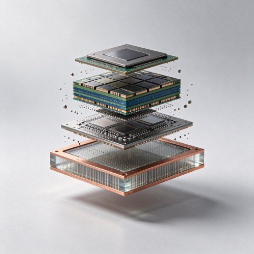
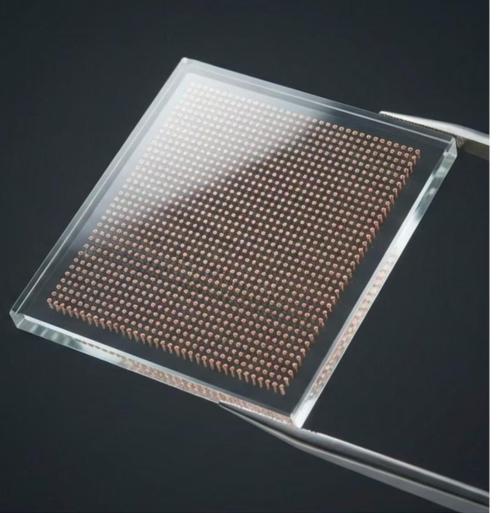
Felix Glass supplies void-free copper filled TGV glass interposers, finished with laser drilled vias, dielectric liner, Ti/Cu seed deposition, electroplated copper fill and CMP planarization. Designed for high-density chiplet integration, this finished interposer is the ready-to-test interconnect platform for AI GPU, HBM stacks, high-speed networking ASIC and 2.5D advanced packaging.
What Is Copper Filled TGV Glass Interposer
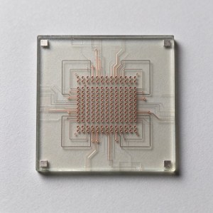
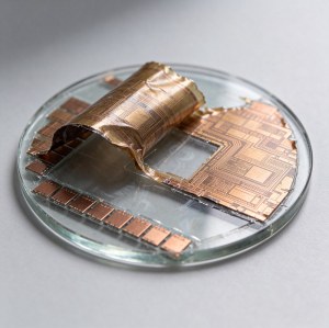
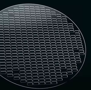
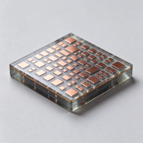
A copper filled TGV interposer is a finished glass interposer substrate with fully metallized, void-free through-glass vias. Starting from double-side polished alkali-free glass, we perform laser via drilling, sidewall cleaning, insulating dielectric liner, barrier and seed layer sputtering, void-free copper electroplating, then CMP to remove overburden copper. Optional single or double-side RDL patterning can be added. Unlike bare glass blanks or drilled-only TGV wafers, this part delivers functional vertical electrical interconnects for your assembly and reliability qualification.
Key Performance Advantages
- Void-free copper via filling, X-ray inspected for internal void and seam defects
- Tunable CTE closely matched to silicon, suppressing thermal warpage during HBM stacking and thermal cycling
- Ultra-low dielectric loss, stable signal integrity for 112Gbps / 224Gbps high-speed interfaces
- Smooth CMP surface, compatible with fine-line RDL, microbump and hybrid bonding process
- Large panel scalability vs silicon TSV interposer, lower cost for large multi-die packages
- Semiconductor-grade metrology reports: TTV, warpage, via position accuracy, sidewall quality, electrical continuity
Standard Technical Specifications
| Parameter | Spec Range |
|---|---|
| Glass Material | Alkali-free aluminosilicate / borosilicate glass |
| Form Factor | 100mm,200mm,300mm wafer, custom panel sizes |
| Glass Thickness | 100μm ~ 700μm |
| TGV Via Diameter | 20μm – 120μm; Aspect ratio up to 10:1 |
| Via Pitch | Minimum 50μm |
| Metallization Stack | Dielectric liner / Ti barrier / Cu seed / Electroplated Cu fill |
| Surface Planarization | CMP post copper fill |
| Flatness | TTV ±5μm standard; ±2μm tight tolerance option |
| Warpage | ≤30μm @300mm wafer after full copper filling and CMP |
| Optional Add-on | Single-side / double-side RDL, NiAu finish |
Manufacturing & Inspection Flow
Process sequence: Double-side polished glass blank → Laser via ablation & cleaning → Dielectric liner deposition → Ti/Cu barrier-seed sputtering → Void-free copper electroplating → CMP planarization → Electrical continuity test → X-ray void inspection → Metrology mapping → Visual defect screening → Packing. Every sample can be supplied with cross-section SEM sampling report for qualification batches. We follow your drawing DFM rules before tooling and flag high-risk geometry at the quotation stage.
Primary Application Areas
- AI GPU 2.5D packaging with HBM memory stacks and chiplet disaggregation
- HPC high performance computing multi-chiplet heterogeneous integration
- High-speed networking ASIC and high-frequency RF interposer test vehicles
- Silicon photonics and co-packaged optics intermediate interconnect substrate
- Semiconductor qualification test coupons for TGV reliability validation
Compare With Drilled-Only TGV Wafer
- Laser Drilled TGV Wafer: Only via holes, no copper filling. For customers owning internal PVD, plating and CMP lines.
- Copper Filled TGV Interposer: Fully finished copper filled vias + CMP. Ready for RDL, bumping and reliability test; reduces your internal fab workload and qualification cycle.
TGV Cluster Navigation
Select other TGV substrate variants matching your process stage:
- TGV Glass Substrate Hub
- Bare polished glass wafer
- Laser drilled TGV glass wafer
- Temporary release glass carrier
- Glass core FC-BGA substrate
- CPO photonic TGV glass substrate
- TGV glass interposer selection guide
- TGV glass wafer engineering design specifications
Request RFQ for Copper Filled TGV Interposer
Submit your stack drawing, via array layout, target glass grade, wafer size/thickness, RDL requirements, surface finish, inspection criteria and quantity breakdown (sample / qualification / volume). Our optical and semiconductor packaging engineers run DFM review and return formal quotation, lead time and risk notes under NDA.
FAQ
Q: Can you guarantee zero void in copper filled TGV?
A: We use optimized bottom-up electroplating process and X-ray 100% screening on acceptance lots to control voids below your specified threshold. Cross-section SEM sampling is available for qualification validation.
Q: Is RDL included as standard?
A: RDL is optional add-on. Standard deliverable is copper filled + CMP planarized interposer without redistribution layer.
Q: What reliability tests can these interposers support?
A: Suitable for thermal cycling, HAST, TCB, high-temperature storage and electrical continuity reliability evaluation for chiplet packaging.
Q: What file format do you accept for via array?
A: Gerber, OASIS, DXF, Excel coordinate list and PDF drawing are all supported for DFM check.
Q: What is typical lead time for engineering samples?
A: Sample lead time depends on via geometry and metrology requirements, we will confirm in formal quotation after drawing review.
Contact TGV Packaging Engineering Team
Share your specification package to get DFM feedback, budget price and sample schedule for copper filled TGV glass interposer.
Request a Quote