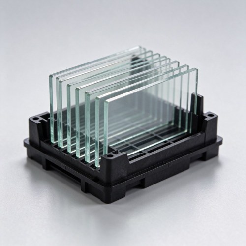
CPO Photonic TGV Glass Substrate
Item specifics
- Glass Material
- Low-Loss Alkali-Free Aluminosilicate Photonic Grade Glass
- Substrate Format
- 100 mm, 200 mm, 300 mm Wafer / Custom Photonic Panels
- Nominal Thickness
- 100–800 µm
- Via Spec
- TGV Via Diameter 20–150 µm
- Optical Band
- 1260–1360 nm O-Band, 1500–1600 nm C-Band
- Application
- Co-Packaged Optics, Silicon Photonics and Photonic-Electronic Integration
Review
Description
CPO Photonic TGV Glass Substrate
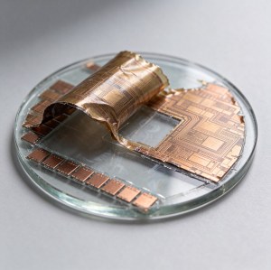
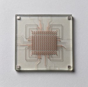
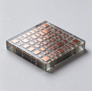
Felix Glass supplies low-loss CPO photonic TGV glass substrates built for co-packaged optics, silicon photonics and high-speed optical engine integration. This glass platform combines electrical through-glass vias and optical transmission performance, supporting hybrid electrical-optical interconnection for next-generation data center and AI hardware.
What Is CPO Photonic TGV Glass Substrate
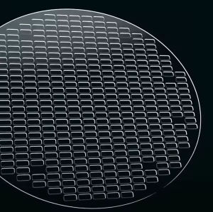
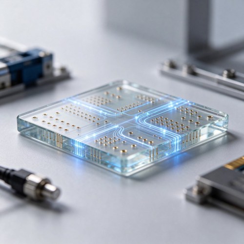
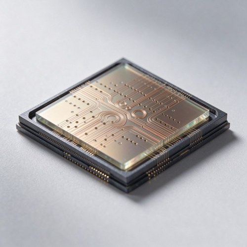
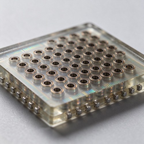
CPO photonic TGV glass substrate is a specialized glass interposer designed for co-packaged optics. It uses low optical-loss alkali-free glass as the base material. Laser-processed TGV vias provide vertical electrical signal paths, while the glass itself acts as a light-transmissive medium for optical coupling, waveguides and fiber attach interfaces. Unlike standard electrical-only TGV interposers, this substrate is optimized to meet both high-frequency electrical and photonic optical requirements for optical engine co-packaging.
Core Advantages
- Low optical absorption at target telecom wavelengths for silicon photonic coupling
- Low dielectric loss, suitable for high-speed electrical signals alongside optical paths
- Precision TGV vias for vertical electrical interconnect, customizable via layout
- High dimensional stability and low CTE, matching silicon photonic die thermal behavior
- Compatible with waveguide patterning, fiber alignment, flip-chip and RDL integration workflows
Product Specifications & Customizable Parameters
| Parameter | Custom Range |
|---|---|
| Base Glass Material | Low-loss alkali-free aluminosilicate photonic grade glass |
| Form Factor | 100/200/300mm wafer, custom photonic panel sizes |
| Substrate Thickness | 100μm ~ 800μm |
| TGV Via Diameter | 20μm ~ 150μm |
| Optical Band | 1260–1360nm O-band, 1500–1600nm C-band |
| Inspection | Optical transmission, via metrology, flatness, surface defects |
Typical Application Scenarios
- Co-packaged optics (CPO) optical engine substrates for AI and data center switches
- Silicon photonics packaging, light coupling and fiber alignment structures
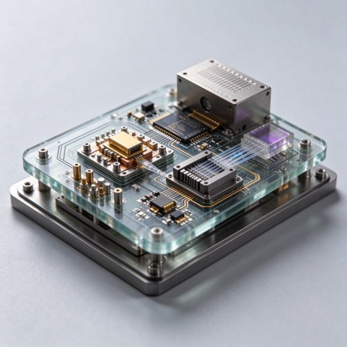
- Hybrid photonic-electronic interposers for high-bandwidth optical I/O
- Photonic integrated circuit (PIC) carrier and test vehicle development
- High-speed transceiver packaging with combined electrical and optical routing
Optical & Electrical Performance Notes
Photonic-grade glass is selected to minimize absorption and scattering at your operating wavelength. We control surface roughness and subsurface damage during polishing to reduce optical coupling loss. TGV structures are optimized for signal integrity at high data rates. Optical transmission test data and electrical S-parameter test reports can be provided for qualification batches. Waveguide writing, grating coupler and fiber array alignment features can be supported on request.
Compare With Our Other TGV Substrates
This substrate is optimized for photonic and CPO hybrid packaging. If you only require electrical interconnection for HBM and AI GPU packaging, see our Copper filled TGV glass interposer. For blank photonic glass without vias, select our Bare Polished Glass Wafer. For pre-drilled vias without metallization, review Laser Drilled TGV Glass Wafer.
Quality Control & Photonic Inspection
Each batch undergoes optical transmission screening, surface defect inspection, TTV, warpage and via geometry measurement. Photonic test coupons can be supplied alongside production wafers for your fiber coupling and insertion loss validation. All substrates are packed in cleanroom containers to avoid contamination that degrades optical performance.
Request Photonic DFM Review & Quotation
Submit your target wavelength, optical coupling scheme, TGV layout, substrate size and quantity. Our engineering team reviews optical and electrical manufacturability and provides sample pricing and lead time for CPO prototype builds.
FAQ for CPO Photonic TGV Glass Substrate
Q: Does this substrate come with integrated optical waveguides?
A: Waveguide patterning is an optional secondary process. Base delivery is polished glass with TGV vias.
Q: Can you provide insertion loss and transmission spectra test reports?
A: Yes, optical performance data can be included with qualification lots.
Q: Is this glass compatible with grating coupler fabrication?
A: Yes, the photonic glass grade is suitable for grating coupler and light coupling structures.
Q: Can I order blank photonic glass without TGV vias first for optical testing?
A: Absolutely, bare photonic glass blanks are available as a separate SKU.
Related TGV Glass Solutions
- Temporary release glass carrier
- Glass core FC-BGA substrate
- TGV glass wafer engineering design specifications
- TGV glass interposer selection guide
Get Quote for CPO Photonic TGV Glass Substrate
Share your CPO stack, wavelength specs and layout files for photonic DFM review, pricing and sample lead time. All photonic design information is protected under NDA.
Request a Quote